


Samsung Electronics pushes the glass substrate to power FOPLP packaging technology
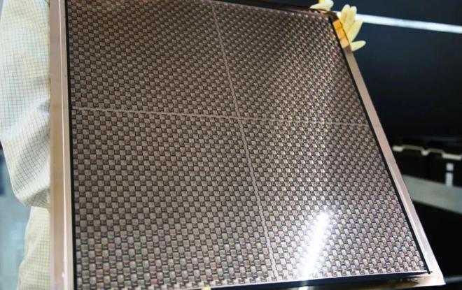
Today, the global electronics industry is booming! Semiconductor technology is also undergoing a new revolution. You see, smartphones, artificial intelligence, and the Internet of Things are developing too fast, and the requirements for chip performance, size, and cost are getting higher and higher, and traditional packaging technology simply cannot meet the needs of the market. At this time, Samsung Electronics put forward an innovative technology - glass substrate FOPLP (Fan-Out Panel Level Packaging) packaging technology, which can become a hot thing for everyone in the industry to compete for.
Let's start with the benefits of this glass substrate. Compared with traditional organic substrates, the physical properties of glass substrates are excellent! First, its coefficient of thermal expansion is low, even in high temperature or high humidity environment, the adhesion between the chip and the substrate is stable, because the damage caused by temperature changes is greatly reduced. And the glass substrate has better light transmission and can support higher density packaging, so that the performance and efficiency of the BZX84B9V1W chip will not rise! Finally, the use of this material can also reduce transmission losses during the packaging process, and the overall performance will be improved.
Let's take a look at the background of this FOPLP packaging technology. As an emerging packaging technology, the power lies in the fact that the position of the chip relative to the substrate can be designed more precisely, resulting in improved functionality and performance. Specifically, FOPLP technology allows many chips to be packaged on the same substrate, which greatly improves space utilization. In the pursuit of miniaturization and thin and light product design, especially in consumer electronics such as smartphones, users like thin and light design, so this FOPLP technology is particularly valued.
Samsung's glass substrate FOPLP packaging technology greatly improves the integrated density of the chip through innovative design, not only better performance, but also greater stability and durability. This technology has been developed in response to the market's constant pursuit of high performance, high integration and high stability, enabling Samsung to continue to maintain its leading position in a highly competitive market.
Let's talk about productivity gains. Samsung Electronics is very active, investing in modernized production lines to support the mass production of FOPLP technology for glass substrates. By introducing and optimizing automated production processes, the company has increased efficiency at every step of the production process. At the same time, Samsung also pays special attention to reducing waste and resource consumption in the production process, and strives to move towards the goal of sustainable development.
In actual production, Samsung uses advanced lithography and etching technology, so higher precision packages and smaller chip arrangements can be achieved. As soon as the efficiency is improved, the production cost will not be reduced, and it can also help enterprises meet the market demand for new products in a short time!
Next, look at the market outlook and competitive strategy. The competition in the semiconductor industry is becoming more and more fierce, and technological innovation has become an important means for enterprises to gain market share and attract customers' attention. The glass substrate FOPLP packaging technology launched by Samsung Electronics is one of Samsung Electronics' strategies to cope with market challenges. By combining the latest packaging technology with its product line, Samsung hopes to further cement its leadership position in the high-end electronics segment.
At the same time, Samsung Electronics continues to expand its relationships with partners in an effort to contribute to the construction of the industrial ecosystem. By working closely with other technology companies, research institutions and customers, Samsung can quickly get market feedback and then improve products accordingly. This flexible strategy not only makes the product more adaptable, but also improves the market competitiveness.
Let's talk about the future direction of technology. While continuing to advance FOPLP technology on glass substrates, Samsung Electronics is not idle, and is also actively exploring other emerging technologies. As an industry leader, Samsung understands that it needs to constantly innovate to remain competitive in the market. As a result, they are investing significant resources in research and development to find those areas of technology that could impact the semiconductor industry in the future. From quantum computing to artificial intelligence, Samsung aims to stay ahead of future technology trends.
In addition, Samsung Electronics is also working on thin film transistors (TFT), micro-electro-mechanical systems (MEMS) and optoelectronics in these areas, and looking for ways to expand the application of its own technology. This comprehensive technical layout allows Samsung to work in many areas at the same time, and the market competitive advantage is more obvious.
Once the glass substrate FOPLP technology was launched, it caused quite a stir in the industry. Some competitors are following suit and accelerating improvements and investments in their own technology. This trend not only allows semiconductor technology to develop faster, but also brings more opportunities for cooperation and competition to the entire industry. Industry experts said that Samsung's innovation is likely to change the ecological landscape of semiconductor packaging technology in the coming years!
In order to cope with market feedback and competitive pressure, Samsung Electronics constantly adjusts its market strategy, actively communicates with large customers, understands their needs and feedback, and then continuously optimizes products and services according to these. By responding so quickly to the market, Samsung has remained flexible in the face of fierce competition and has been able to get closer to key customers.
As the global demand for electronic products continues to increase, Samsung Electronics' glass substrate FOPLP packaging technology will continue to show its potential in many areas. The market's pursuit of higher product performance and smaller size will certainly promote the rapid development and wide application of this technology. Although facing challenges from inside and outside the industry, Samsung Electronics will continue to lead the competition in the future with its own technical strength and market insight.
The Products You May Be Interested In
 |
AISC-1210-68NJ-T | FIXED IND 68NH 900MA 150 MOHM | 4086 More on Order |
 |
AMPMGDA-12.5000T3 | MEMS OSC XO 12.5000MHZ CMOS SMD | 7488 More on Order |
|
AMPMDEB-5.1200T3 | MEMS OSC XO 5.1200MHZ CMOS SMD | 6228 More on Order |
|
AMPMDGC-45.0000T | MEMS OSC XO 45.0000MHZ CMOS SMD | 6246 More on Order |
|
AMPMEEC-62.5000 | MEMS OSC XO 62.5000MHZ CMOS SMD | 6606 More on Order |
|
AMPMDEC-11.0590 | MEMS OSC XO 11.0590MHZ CMOS SMD | 3150 More on Order |
 |
ABDFTCXO-10.000MHZ-E-2-T2 | XTAL OSC TCXO 10.0000MHZ LVCMOS | 5184 More on Order |
 |
AOCJY-40.000MHZ-E | XTAL OSC VCOCXO 40.0000MHZ CMOS | 6768 More on Order |
|
AX5PAF4-1200.0000T | OSC XO 1.2GHZ 3.3V LVPECL | 5526 More on Order |
 |
AX7MCF3-700.0000T | XTAL OSC XO 700.0000MHZ CML SMD | 6948 More on Order |
 |
ASG-C-V-B-125.000MHZ | XTAL OSC VCXO 125.0000MHZ LVCMOS | 8154 More on Order |
 |
AX7DCF4-156.2500C | XTAL OSC XO 156.2500MHZ LVDS SMD | 2754 More on Order |
 |
ASG2-P-V-B-698.812334MHZ-T | XTAL OSC VCXO 698.812334MHZ LVPE | 7146 More on Order |
|
AX5MCF1-173.3708C | OSC XO 173.370781MHZ 1.8V CML | 7128 More on Order |
 |
AX7DBF1-164.3555T | XTAL OSC XO 164.3555MHZ LVDS SMD | 8064 More on Order |
|
ABM13W-60.0000MHZ-8-K2Z-T5 | CRYSTAL 60MHZ 8PF SMD | 3690 More on Order |
|
ABM13W-45.0000MHZ-5-JH7Z-T5 | CRYSTAL 45MHZ 5PF SMD | 2106 More on Order |
 |
ABM2-33.000MHZ-D4YF-T | CRYSTAL 33.0000MHZ 18PF SMD | 3078 More on Order |
 |
ABS04W-32.768KHZ-6-B5-T5 | CRYSTAL 32.768KHZ 6PF SMD | 5382 More on Order |
 |
ABM11W-30.3200MHZ-4-K1Z-T3 | CRYSTAL 30.3200MHZ 4PF SMD | 4212 More on Order |
 |
ABM10W-38.4000MHZ-4-J1Z-T3 | CRYSTAL 38.4000MHZ 4PF SMD | 4518 More on Order |
 |
ABM8W-48.0000MHZ-8-J2Z-T3 | CRYSTAL 48.0000MHZ 8PF SMD | 4716 More on Order |
 |
ABM10W-24.5454MHZ-7-B1U-T3 | CRYSTAL 24.5454MHZ 7PF SMD | 8946 More on Order |
 |
ABM3-12.288MHZ-D2Y-T | CRYSTAL 12.2880MHZ 18PF SMD | 118758 More on Order |