


NTLJD3181PZTBG Datasheet

|
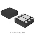
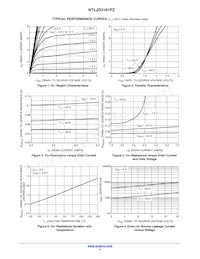
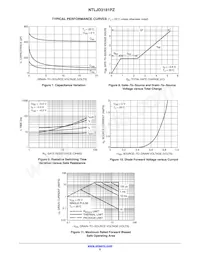
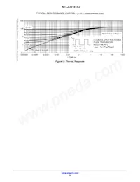
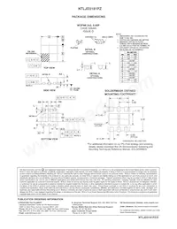
Manufacturer ON Semiconductor Series - FET Type 2 P-Channel (Dual) FET Feature Logic Level Gate Drain to Source Voltage (Vdss) 20V Current - Continuous Drain (Id) @ 25°C 2.2A Rds On (Max) @ Id, Vgs 100mOhm @ 2A, 4.5V Vgs(th) (Max) @ Id 1V @ 250µA Gate Charge (Qg) (Max) @ Vgs 7.8nC @ 4.5V Input Capacitance (Ciss) (Max) @ Vds 450pF @ 10V Power - Max 710mW Operating Temperature -55°C ~ 150°C (TJ) Mounting Type Surface Mount Package / Case 6-WDFN Exposed Pad Supplier Device Package 6-WDFN (2x2) |
Manufacturer ON Semiconductor Series - FET Type 2 P-Channel (Dual) FET Feature Logic Level Gate Drain to Source Voltage (Vdss) 20V Current - Continuous Drain (Id) @ 25°C 2.2A Rds On (Max) @ Id, Vgs 100mOhm @ 2A, 4.5V Vgs(th) (Max) @ Id 1V @ 250µA Gate Charge (Qg) (Max) @ Vgs 7.8nC @ 4.5V Input Capacitance (Ciss) (Max) @ Vds 450pF @ 10V Power - Max 710mW Operating Temperature -55°C ~ 150°C (TJ) Mounting Type Surface Mount Package / Case 6-WDFN Exposed Pad Supplier Device Package 6-WDFN (2x2) |