


NTB13N10G Datasheet

|
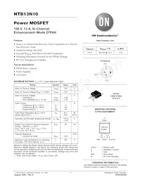
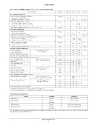
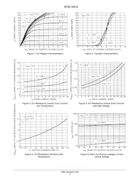
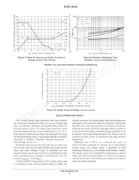
Manufacturer ON Semiconductor Series - FET Type N-Channel Technology MOSFET (Metal Oxide) Drain to Source Voltage (Vdss) 100V Current - Continuous Drain (Id) @ 25°C 13A (Ta) Drive Voltage (Max Rds On, Min Rds On) 10V Rds On (Max) @ Id, Vgs 165mOhm @ 6.5A, 10V Vgs(th) (Max) @ Id 4V @ 250µA Gate Charge (Qg) (Max) @ Vgs 20nC @ 10V Vgs (Max) ±20V Input Capacitance (Ciss) (Max) @ Vds 550pF @ 25V FET Feature - Power Dissipation (Max) 64.7W (Ta) Operating Temperature -55°C ~ 175°C (TJ) Mounting Type Surface Mount Supplier Device Package D2PAK Package / Case TO-263-3, D²Pak (2 Leads + Tab), TO-263AB |
Manufacturer ON Semiconductor Series - FET Type N-Channel Technology MOSFET (Metal Oxide) Drain to Source Voltage (Vdss) 100V Current - Continuous Drain (Id) @ 25°C 13A (Ta) Drive Voltage (Max Rds On, Min Rds On) 10V Rds On (Max) @ Id, Vgs 165mOhm @ 6.5A, 10V Vgs(th) (Max) @ Id 4V @ 250µA Gate Charge (Qg) (Max) @ Vgs 20nC @ 10V Vgs (Max) ±20V Input Capacitance (Ciss) (Max) @ Vds 550pF @ 25V FET Feature - Power Dissipation (Max) 64.7W (Ta) Operating Temperature -55°C ~ 175°C (TJ) Mounting Type Surface Mount Supplier Device Package D2PAK Package / Case TO-263-3, D²Pak (2 Leads + Tab), TO-263AB |
Manufacturer ON Semiconductor Series - FET Type N-Channel Technology MOSFET (Metal Oxide) Drain to Source Voltage (Vdss) 100V Current - Continuous Drain (Id) @ 25°C 13A (Ta) Drive Voltage (Max Rds On, Min Rds On) 10V Rds On (Max) @ Id, Vgs 165mOhm @ 6.5A, 10V Vgs(th) (Max) @ Id 4V @ 250µA Gate Charge (Qg) (Max) @ Vgs 20nC @ 10V Vgs (Max) ±20V Input Capacitance (Ciss) (Max) @ Vds 550pF @ 25V FET Feature - Power Dissipation (Max) 64.7W (Ta) Operating Temperature -55°C ~ 175°C (TJ) Mounting Type Surface Mount Supplier Device Package D2PAK Package / Case TO-263-3, D²Pak (2 Leads + Tab), TO-263AB |