


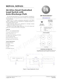
NCP434FCT2G Datasheet

|
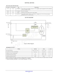
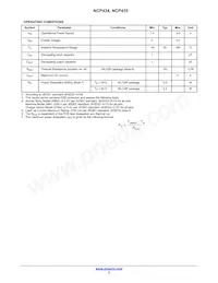
Manufacturer ON Semiconductor Series - Switch Type General Purpose Number of Outputs 1 Ratio - Input:Output 1:1 Output Configuration High Side Output Type P-Channel Interface On/Off Voltage - Load 1V ~ 3.6V Voltage - Supply (Vcc/Vdd) Not Required Current - Output (Max) 2A Rds On (Typ) 65mOhm Input Type Non-Inverting Features Slew Rate Controlled Fault Protection - Operating Temperature -40°C ~ 85°C (TA) Package / Case 4-UFBGA, WLCSP Supplier Device Package 4-WLCSP (0.96x0.96) |
Manufacturer ON Semiconductor Series - Switch Type General Purpose Number of Outputs 1 Ratio - Input:Output 1:1 Output Configuration High Side Output Type P-Channel Interface On/Off Voltage - Load 1V ~ 3.6V Voltage - Supply (Vcc/Vdd) Not Required Current - Output (Max) 2A Rds On (Typ) 65mOhm Input Type Non-Inverting Features Load Discharge, Slew Rate Controlled Fault Protection - Operating Temperature -40°C ~ 85°C (TA) Package / Case 4-UFBGA, WLCSP Supplier Device Package 4-WLCSP (0.96x0.96) |