


ADP197ACBZ-R7 Datasheet


|
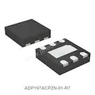
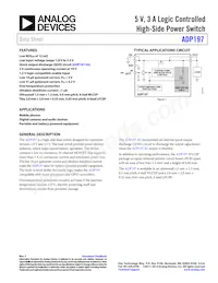
Manufacturer Analog Devices Inc. Series - Switch Type General Purpose Number of Outputs 1 Ratio - Input:Output 1:1 Output Configuration High Side Output Type N-Channel Interface On/Off Voltage - Load 1.8V ~ 5.5V Voltage - Supply (Vcc/Vdd) Not Required Current - Output (Max) 3A Rds On (Typ) 12mOhm Input Type Non-Inverting Features Slew Rate Controlled Fault Protection Over Temperature Operating Temperature -40°C ~ 105°C (TJ) Package / Case 6-WFBGA, WLCSP Supplier Device Package 6-WLCSP (1.45x0.95) |
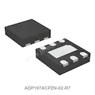
Manufacturer Analog Devices Inc. Series - Switch Type General Purpose Number of Outputs 1 Ratio - Input:Output 1:1 Output Configuration High Side Output Type N-Channel Interface On/Off Voltage - Load 1.8V ~ 5.5V Voltage - Supply (Vcc/Vdd) Not Required Current - Output (Max) 3A Rds On (Typ) 27mOhm Input Type Non-Inverting Features Slew Rate Controlled Fault Protection Over Temperature Operating Temperature -40°C ~ 105°C (TJ) Package / Case 6-UDFN Exposed Pad, CSP Supplier Device Package 6-LFCSP-UD (2x2) |
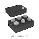
Manufacturer Analog Devices Inc. Series - Switch Type General Purpose Number of Outputs 1 Ratio - Input:Output 1:1 Output Configuration High Side Output Type N-Channel Interface On/Off Voltage - Load 1.8V ~ 5.5V Voltage - Supply (Vcc/Vdd) Not Required Current - Output (Max) 3A Rds On (Typ) 27mOhm Input Type Non-Inverting Features Load Discharge, Slew Rate Controlled Fault Protection Over Temperature Operating Temperature -40°C ~ 105°C (TJ) Package / Case 6-UDFN Exposed Pad, CSP Supplier Device Package 6-LFCSP-UD (2x2) |
Manufacturer Analog Devices Inc. Series - Switch Type General Purpose Number of Outputs 1 Ratio - Input:Output 1:1 Output Configuration High Side Output Type N-Channel Interface On/Off Voltage - Load 1.8V ~ 5.5V Voltage - Supply (Vcc/Vdd) Not Required Current - Output (Max) 3A Rds On (Typ) 12mOhm Input Type Non-Inverting Features Slew Rate Controlled Fault Protection Over Temperature Operating Temperature -40°C ~ 105°C (TJ) Package / Case 6-WFBGA, WLCSP Supplier Device Package 6-WLCSP (1.45x0.95) |